What is Heavy Copper PCB?
Typically, most PCBs are manufactured using copper thicknesses ranging from 1oz to 3oz.However,a heavy copper PCB refers to a PCB where 3oz or greater copper is used on all layers of the board (both inner and outer layers).

Why Heavy Copper PCBs are Used?
Some PCBs are designed to carry higher current levels (amperage) by using wider traces. However, as power requirements increase, thicker copper is needed to transmit signals across the board.This is why heavy copper PCBs are used in high current designs.
The Advantages of Heavy Copper PCB
• Improved thermal performance: Heavy copper PCBs can withstand repeated thermal cycles during manufacturing and assembly processes.
• Increased current carrying capacity: Heavy copper PCBs offer better electrical conductivity and can handle higher current loads. Increasing the copper trace width can enhance the current carrying capacity, and thicker copper traces can handle even larger current loads.
• Increased mechanical strength: Heavy copper PCBs enhance mechanical strength at connectors and plated-through holes, ensuring the board's structural integrity and making the electrical system more robust and resistant to voltage.
• Excellent dissipation factor: Heavy copper PCBs are highly suitable for large power-loss components. These PCBs can prevent electrical systems from overheating and effectively dissipate heat.
• Good conductor: Heavy copper PCBs are good conductors, making them useful in the production of electronic products. They help to connect various boards together, which can transmit currents.
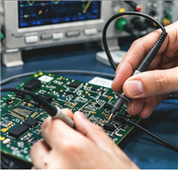
Capabilities of Heavy Copper PCB
As a PCB service provider with over a decade of experience in PCB manufacturing and PCB assembly, PCBWay has a rich background in manufacturing heavy copper PCB. Check our capabilities in the following table:
| Feature | Capability |
| Material | FR-4 Standard Tg 140°C, FR4-High Tg 170°C |
| Min.Track/Spacing |
For External layers: 4oz Cu 13mil/13mil,5oz Cu 18mil/18mil 6oz Cu 18mil/18mil,12oz Cu 20mil/32mil |
For Internal layers:
4oz Cu 13mil/13mil,5oz Cu 18mil/18mil 6oz Cu 18mil/18mil,12oz Cu 20mil/32mil |
| Min.Hole Size | 10mil |
| Max Outer Layer Copper Weight(Finished) | 15oz |
| Max Inner Layer Copper Weight | 12oz |
| Board Thickness | 0.6-6mm |
| Surface Finishing | HASL lead free,Immersion gold,OSP,Hard Gold,Immersion Silver,Enepig |
| Solder Mask | Green,Red,Yellow,Blue,White,Black,Purple, Matte Black,Matte green |
| Silkscreen | White,Black |
| Via Process | Tenting Vias,Plugged Vias,Vias not covered |
| Testing | Fly Probe Testing (Free) and A.O.I.testing |
| Build time | 5-10 days |
| Lead time | 2-3 days |
Applications of Heavy Copper PCB
Heavy copper PCBs are becoming more and more popular due to their wide application in the following fields:
• Military: Weapons control, radar, and monitoring systems.
• Automotive industries: Rail track system and signal transmission system.
• Power distribution: Excitation systems for power regulators, power grid switching systems, high power rectifiers, and overload relays.
• Transportation: Power converters for railway systems, power line monitors, traction converters.
• Industrial controls: Safety and signal systems, welding equipment, protection relays, surge protectors.
• Renewable Systems: Power converters, energy storage, power grid back-up, hydroelectric power plants control panels.
PCBWay provides services including PCB Prototype & Batch Production, PCB Assembly (SMT), Electronics Modules Selling, CNC Machining, etc. We are committed to meeting the needs of global makers from different industries in terms of quality, delivery, cost-effectiveness and any other demanding requests in electronics.
More information please check here:
Heavy Copper PCB Instant Quote