Bypass Capacitor
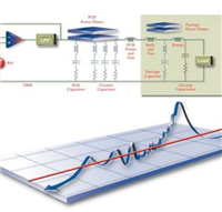
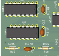
A capacitor which provides a comparatively low impedance ac (alternating current ) around a circuit element.
Bus
A heavy trace or conductive metal strip on the printed circuit board used to distribute voltage, grounds, etc., to smaller branch trances.
Bus Bar
A conduit, such as a conductor on a printed board, for distributing electrical energy.
Burn-in
A method of testing devices via electrical stress vs temperature and/or time so that units prone to failure are eliminated.
Buried Via
A via that does not reach a surface layer on either side of a multi-layer board. The via transcends only inner layers of the board.
Bulge
A swelling of a printed board that is usually caused by internal de-lamination or separation of fibres.
B-stage
( prepreg ) Partially cured resin ( mostly reinforced with glass cloth ) which will soften under a special range of temperature and which can be used to bond together cured laminate sheets to form a multi-layer board.
B-stage Resin
A resin in an intermediate state of cure. The cure is normally completed during the laminating cycle.
Bridging
A condition where excess solder builds up in the air gap between conductors and causes them to short together. Solder bridging generally occurs during the wave soldering process. Bridging is basically short-circuiting of a pad to an adjacent track or pad on a board.
Bridged Joint
Solder that spans across two or more conductors causing an electrical short-circuit.
Breakdown Voltage
The voltage at which an insulator or dielectric ruptures or at which ionization and conduction take place in a gas or vapour.
Brazing Alloy
A metal alloy (solder) which melts above 450℃ but below metals being joined.
Branched Conductor
A conductor which connects electrically two or more leads on a printed board assembly. Some branched conductors, notably ground, support and re-set signal, connect many leads.
Bow
The deviation from the flatness of a board characterized by a roughly cylindrical or spherical curvature. If the board is rectangular, its four corners are in the same plane (see also: “twist’).
Boundary Scan
A self-test designed into components at the silicon level, permitting testing via a built-in, four-or-five-pin test bus accessing I/O pins.
Border Data
Patterns that appear in the border area, such as tooling features, test patterns and registration marks.
Bonding Time
The duration from hot-bar-heat-up (contact with lead and pad ) until the solder joint is completed.
Bonding Layer
An adhesive layer used in bonding together other discrete layers of multi-layer printed board during lamination.
Bond Strength:
The force perpendicular to a board’s surface required to separate two adjacent layers of the board, expressed as force pre unit area.
Bond Lift-off
A failure condition in which a lead is separated from its bonding surface.
Bond Interface
The common area between a lead and a land to which it has been terminated.
Body
The portion of an electronic component exclusive of its pins or leads.
Board Thickness
The overall thickness of the base material and all conductive materials deposited thereon.
Board Density
A measure of the ratio of the area of the board used by parts to the total available area of the board. A board with less than 50 to 60 per cent of the available area should be able to be done single-sided, more than 75 to 80 per cent may have to go to multi-layer.
Blutter Coat
An external layer of resin over the reinforcing structure of base material.
Bluetooth
Bluetooth is a short-range (up to 10m) 2.4GHz wireless connectivity standard intended for such applications as wireless personal area networks (PANs). These PANs can be used to exchange data between devices such as cellphones, digital cameras, printers and household appliances at data rates of up to 721 Kbps ( kilo bits per second ).
Blow Hole
A void in the solder fillet caused by outgassing from the barrel of a plated through hole.(see also outgassing )
Blistering
A localized swelling and separation between any of the layers of a laminated base material, or between base material and conductive foil. It is a form of de-lamination. Also separation of solder mask layer and conductive pattern.
Blister
De-lamination in the form of a localized swelling and separation between any of the Layers of a lamination base material, or between base material and conductive foil or protective coating.
Blind Via
A via that reaches only one layer beneath the outer layer on one side of a muti-layer board.
Bleeding
A condition in which liquid solder resist or rotation spreads larger than the defined apperture.
Biscuit Frame
An array of circuits on a larger “mother” panel.
BGA
Ball Grid Array. Leadless array packaging technology in which solder balls are mounted to the underside of the package.
Bellows Contact
A connector contact which is a flat sprint folded to provide a uniform spring rate over the full tolerance range of the mating unit.
Bed-of-Nails
A method of PCB testing involving a fixture containing a field of spring-loaded pins that are co-ordinated with strategic points or nodes on the board to which they are brought into contact.
BBT
Bare Board Test.
Basic Wettability
The ease with which a metal or metal alloy can be wetted by molten solder.
Base Solderability
The ease with which a metal or metal alloy surface can be wetted by molten solder under minimum realistic conditions.
Base Material
The insulating material (either rigid or flexible ) as well as the copper foils bonded on one or both sides. It is a synonym for copper-clad laminate, i.e., the basic raw material for PCB manufacture. This also supports all components after assembly.
Base Material Thickness
The thickness of the base material, excluding metal foil or material deposited on the surface.
Base Laminate
The substrate material upon which the conductive wiring pattern may be formed.
Base Copper
The original, thin copper foil present on one or both sides of a copper clad laminate. During PCB manufacture, part of this base copper will be removed by etching. Conductors on the simplest PCBs consist of base copper only.
Barrel
The cylinder formed by plating through a drilled hole.
Bare Board
A PCB having all lines, pads and layers intact but without components installed. An unassembled PCB.
Backpanel (Backplane)
see ”Mother Board”
Backdriving
An in-circuit test procedure for digital circuitry.
B&B
Blind and Buried via holes.
B-stage Material
Laminate impregnated with a resin and cured to an intermediate stage (B-stage resin ). Normally designated as prepreg.


