What is a Fiducial Mark and How Does it Work?
A fiducial mark is typically a circular pad or other shapes of exposed copper that is surrounded by a clearance area. It acts as a reference point for automated machines, such as pick-and-place machines, and also for PCB stencil alignment to ensure that components are accurately placed on the board. During the assembly process, these machines use computer vision systems that scan for the fiducial marks and use their locations to align the PCB and components. Fiducial marks are particularly useful for surface-mount technology components, and it’s advisable to put a mark near the packages with small pitches like BGA, QFN, and QFP.
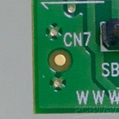
Figure1: Fiducial Mark
Types of Fiducial Marks
There are two types of fiducial marks commonly found in PCB designs: global fiducial marks and local fiducial marks.
Global fiducial marks, also called panel fiducials, are usually placed near the corners of the PCB or on the panelization rails that hold multiple PCBs together during the assembly process.
Local fiducial marks are typically smaller than global fiducial marks and are placed in areas with high-density components or complex routing. By using local fiducial markers, the assembly machines can precisely locate the footprint of a component and reduce errors in fiducial placement.
Generally, it is recommended to have at least two global fiducial marks, one in the lower left corner of the board and one in the upper right corner of the board, placed on a three-point grid-based system.
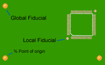
Figure2: Global Fiducial Mark and Local Fiducial Mark
Advantages of Using Fiducial Marks for PCB Assembly
While there are other drilled holes or patterns on the PCB, they may not be suitable for alignment due to inconsistencies in size, shape, or position, which can result in inaccuracies during component placement. Furthermore, these holes or patterns may be covered by the solder mask or silkscreen which makes them difficult to be detected. In contrast, fiducial marks are designed with standardized shapes, sizes, and positions to ensure a clear and consistent reference point for alignment.
Guidelines for Using Fiducial Marks in PCB Design
When adding fiducial marks in your PCB designs, there are a few important guidelines you should consider about.
First, the diameter of the fiducial marks should be consistent throughout the PCB design to ensure accurate alignment. The diameter of a fiducial mark typically ranges from 1 to 3 mm.
Second, if your PCB design has components on both sides, it's important to include fiducial marks on both of them. The absence of fiducial marks on the second side can pose challenges for the automated equipment while flipping the board to assemble components on the opposite side.
Third, the fiducial mark should be free from solder masks and any other coatings. This ensures that the mark is easily visible and distinguishable from the surrounding materials, allowing for accurate and reliable detection by automated assembly equipment.


